

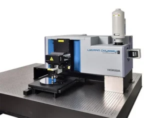
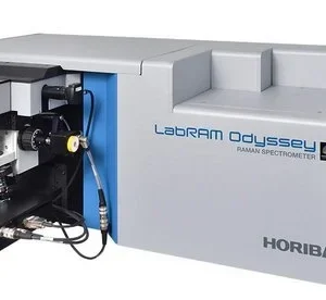
The LabRAM Odyssey Semiconductor microscope is the ideal tool for photoluminescence and Raman imaging on wafers up to 300 mm diameter. The HORIBA best-seller true confocal microscope is equipped with automated 300 mm sample stage and objective turret to fit both needs of wafer uniformity assessment and defects inspection.
FEATURES:
LabRAM Odyssey Semiconductor includes hardware and software designed for semiconductors analysis:
- Wafer mapping with automated turret and sample stage
The automated 300 mm × 300 mm XY sample stage accepts wafers up to 300 mm (12″) diameter for Raman and Photoluminescence mapping of both full wafers and small regions of interest (ROI). The travel speed of the stage together with its stability ensure fast and reliable measurements over ROIs spread over the wafer surface. - Uniformity measurement with wafer tilt correction
The “Tilt at midway” autofocus function corrects for any wafer bow and tilt, producing accurate whole wafer uniformity data, even from thin layers. This function is rapid since it determines the optimum focus height at only at five points prior to mapping: in the center and four points at midway between the center and the corners. - From full wafer to high resolution defect mapping with DuoScan™
DuoScan™ confocal imaging technology is a confocal imaging mode with both capabilities of variable size laser macro-spot scanning (using ultra-fast rastering mirrors) and high precision sub-micron step scanning. Macro-spot scanning is suitable for full wafer mapping while sub-micron step scanning is adapted to defect analysis. - PL and Raman metrology in one tool
The availability of many excitation lasers together with the wide spectral range of the system, from deep UV to near IR, allows simultaneous measurement of photoluminescence and Raman signals in the same spectrum. PL and Raman in one tool significantly speeds up wafer characterization. - Methods: Easy recipe building for highly efficient characterization
Methods will allow you to fully automate your entire Raman/PL characterization routine (acquisition, data processing, display, and analysis) providing high throughput that is manageable by metrology technicians.
The “methods” building process is simple and intuitive : the process or metrology engineer can optimize each operation and in one click insert it into the recipe/method. Individual operations can be conveniently reordered, added or removed.
This customization module is also aided by “templates” which is a way to save and recall a set of hardware configurations and software options. - ParticleFinder PF3: Automated particle characterization
PF3 rapidly locates and chemically characterizes contaminants on a full wafer.
PF3 automatically locates and Raman maps contamination particles. Also PF3 automatically identifies and classifies all detected impurities according to their chemical characteristics (organic, silicon, etc.).
Statistics of morphological properties (area, perimeter, diameter, circularity, brightness, volume estimation, etc.) are also reported.
Related products
-
-
 Laboratory
DIGITAL INCUBATOR + OVERLOAD
-
-
 Laboratory
DIGITAL HEATING MANTLE + STIRRER